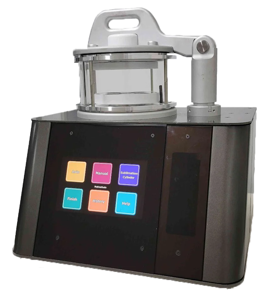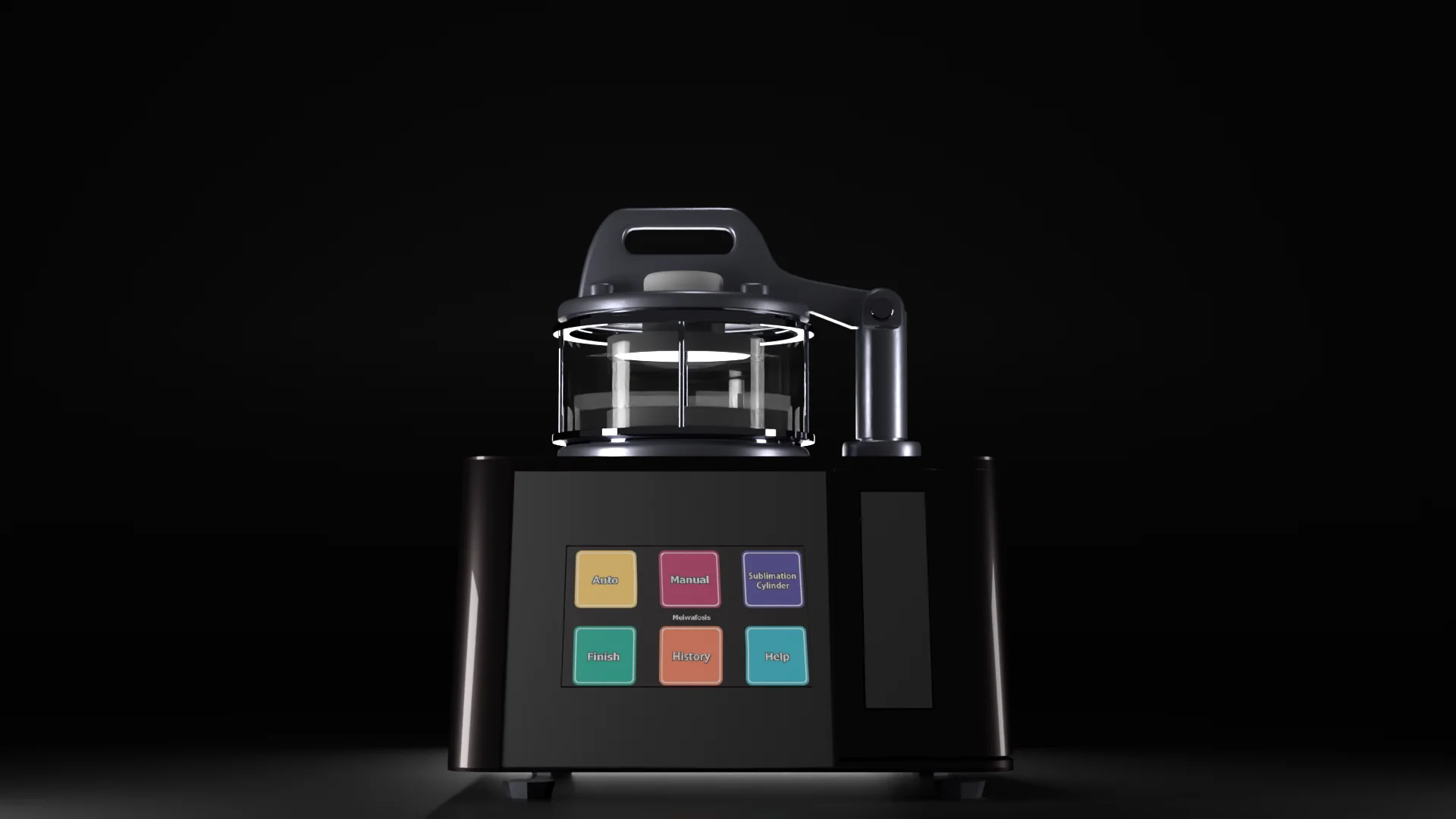
Tennant20 Osmium Coating System

Meiwafosis Co., Ltd. | Made in Japan

Tennant20 — Osmium Coating System

Discovery awaits beneath
an ultra-thin veil

Breaking through the limits of conventional SEM imaging —the Tennant20 Osmium Coating System, engineered in Japan.
Eliminating the granular noise associated with gold coating, it enables clear, artifact-free imaging without charging, revealing the true morphology of nanostructures.

Enter your name and email address to receive a download link.

Scroll
Revealing the true surface with osmium.

Drag the slider to compare.

Accel. Voltage 1.0 kV Magnification 30,000× Os Thickness 5 nm

Data: SHIRAISHI CENTRAL LABORATORIES CO., LTD.

Pt Sputter Coating Osmium Coating (Tennant20)

The nanostructures hidden by gold coating—now revealed.

What is Osmium Coating?

Plasma CVD Osmium Coating

Osmium coating applies plasma CVD technology, refined through decades of use in the semiconductor industry, to deposit metallic osmium films with nanometer-scale thickness control. The process forms a highly uniform conductive film at low temperatures with exceptional thickness reproducibility.

By minimizing charging during SEM imaging and elemental analysis, it enables high-resolution observation of fine surface structures with remarkable clarity.

Tennant20 負グロー相領域

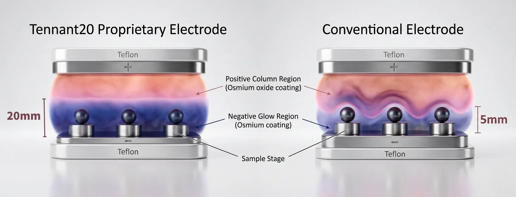
A Larger Negative Glow Region Means Better Coating Quality.

Metallic osmium deposition occurs only within the negative glow region. With conventional parallel-plate electrodes, this region extends only 5 mm above the center of the sample stage.

The Tennant20 features a specially engineered electrode design that expands the negative glow region to 20 mm in height. This enables stable, uniform osmium film deposition even on samples with significant height variations.

Negative Glow Region
Tennant20
20mm
Conventional Electrode
5mm

Clarity Speaks.

Charging Hides What Matters.

Charging

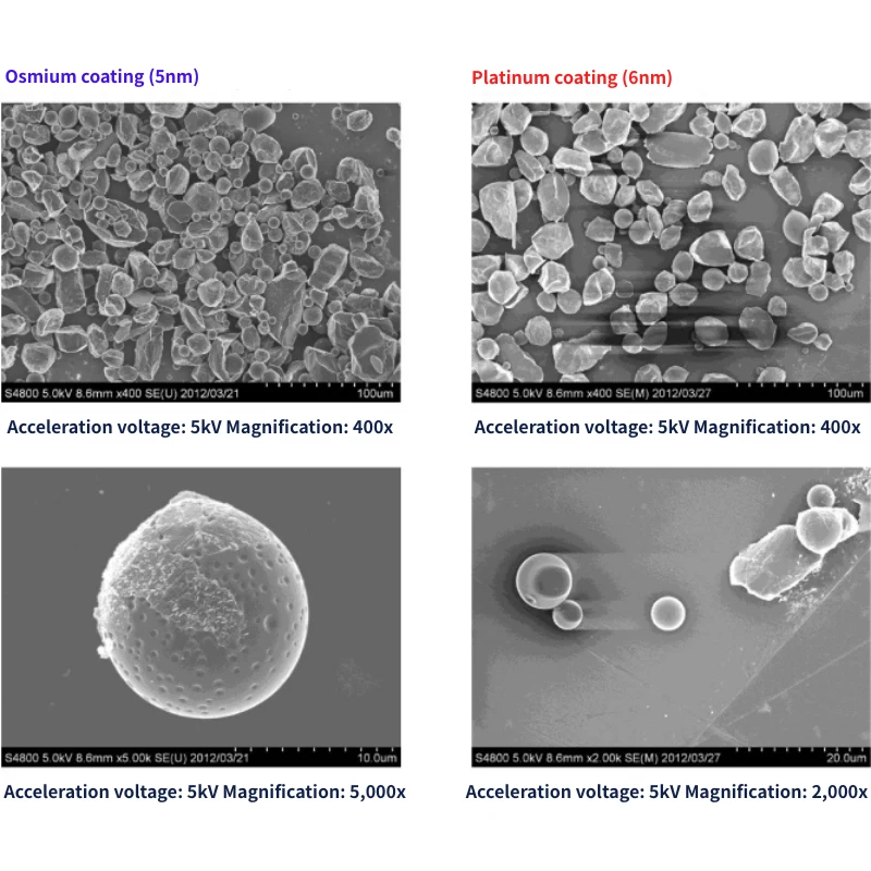
Sputter coating often leads to charging because conductive coverage can be insufficient on complex surfaces.
In contrast, osmium coating provides excellent conductivity, minimizing charging and enabling clear imaging even within complex geometries.

Polystyrene particles comparison: Osmium vs Platinum coating
Hover to zoom.

Our osmium coating systems provide excellent coating coverage, even on overlapping samples, effectively preventing charging and enabling high-contrast observation of the entire sample. On the other hand, gold sputtering often results in charging, particularly in overlapping areas due to poor coating. This limits the maximum magnification to around 2000x. However, osmium coating allows for high-resolution imaging even at 5000x, revealing fine details.

Data provided by Toyohashi University of Technology, Electronic Materials Course, Hiroyuki Muto

Gold Was Hiding the Surface.

Granular Noise

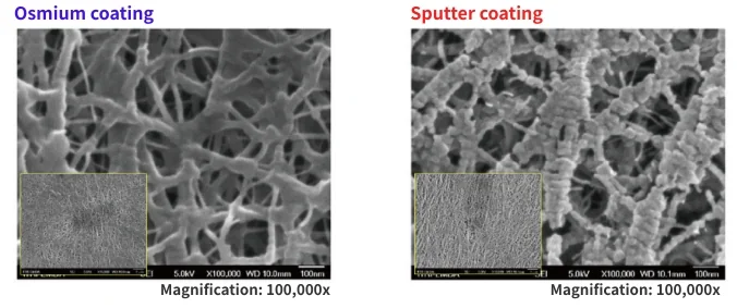
Under gold sputter coating, much of the visible texture can originate from the coating itself rather than the sample.
Osmium coating produces virtually no grain-related artifacts. Even at 150,000× magnification, it reveals the sample surface as it truly is.

Polymer films comparison
Hover to zoom.

Polymer films

At 100,000x, osmium coating provides a smooth surface without any granular artifacts, allowing for clear observation of the true surface structure. In contrast, platinum coating results in a granular surface, obscuring the underlying structure. Osmium coating enables high-resolution imaging without the granular artifacts commonly associated with platinum coating. Additionally, the low applied voltage prevents heat damage to organic samples.
Data provided by Industrial Technology Research Institute (Taiwan)

Meant to coat. Not to damage.

Thermal Damage

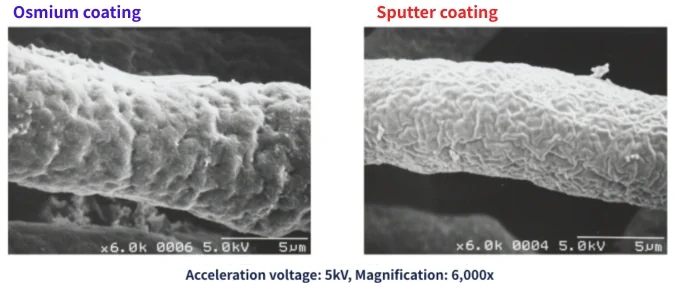
Sputter coating can introduce thermal damage during the coating process.
With a deposition time of only 20 seconds, osmium coating minimizes thermal exposure, preserving the original sample morphology and enabling observation of the sample in its original state.

Rat heart vascular casts comparison
Hover to zoom.

Comparative imaging of rat heart vascular casts

Gold sputtering requires approximately 3 minutes of coating to minimize charging, and this prolonged process often results in heat damage, causing shrinkage and a thick, uneven coating that can obscure fine surface details. In contrast, osmium coating produces a thin, uniform film in just 20 seconds, eliminating charging artifacts and enabling high-resolution imaging of the sample's true morphology. At 6,000x, the difference in surface morphology between the two coating methods is evident. Data provided by Okayama University, Graduate School of Medicine, Dentistry and Pharmaceutical Sciences, Department of Human Morphology

Design Shapes Results.

The Tennant20 was designed to overcome the inherent limitations of conventional osmium coaters.
Three core technologies maximize reproducibility and precision.

Tennant20 製品外観

Proprietary Teflon-Insulated Electrode

By insulating the perimeter of the electrode with Teflon, the negative glow region—where the Os film forms—is expanded to 20 mm above the sample stage (compared to just 5 mm in conventional models). This expanded region enables uniform coating across a larger number of samples in a single run.

Reproducibility

Consistent results, regardless of who operates the system. High-speed feedback control corrects current fluctuations every millisecond, while timer control with 0.01-second resolution enables precise control of ultra-thin films from 0.5 nm upward. By minimizing process variability, the Tennant20 delivers stable and reproducible coating results.

Safety

Engineered for complete gas control. A fully sealed system and automated exhaust sequence effectively manage residual gas within the chamber. After coating is complete, the chamber atmosphere is automatically purged and replaced with clean air. Dedicated solenoid valves automatically close during power interruptions, helping prevent accidental gas leakage.

From 0.5nm
Film Thickness
Nano-level precision control
20mm
Negative Glow Region
4x higher than conventional models
20sec
Deposition Time
Minimizes thermal damage
1ms
Feedback Control
Maintains constant current

Specifications & Quality

Research-grade precision in a compact footprint.
Every design detail reflects the quality of Japanese engineering.

Specifications

Deposition MethodPlasma CVD (Negative Glow Region)
Minimum Film Thickness0.5 nm
Thickness Control (Auto)Target Thickness Setting in 0.1 nm Increments
Thickness Control (Manual)Timer (0.1 s resolution) and current setting
Sample Capacity within the Negative Glow Regionφ10 mm x 15 / φ15 mm x 10 / φ30 mm x 5
Chamber Dimensionsφ150 × 70 mm
External Dimensions (W×D×H)390 x 385 x 435 mm
Weight22 kg
Power SupplyAC 100 V, Max. 10 A
Max. Power Consumption1 kW
User Interface7-inch Touchscreen with Recipe Management
Usage History LogStores up to 500 records
Country of OriginJapan
Made in Japan

Designed and manufactured in Japan by Meiwafosis Co., Ltd., the Tennant20 is backed by rigorous quality control and responsive service support.

Key Specifications

  • PID Feedback Current Control (Proprietary Algorithm)
  • Automated Post-Coating Exhaust Sequence (Standard)
  • Fully Sealed System with Metal Sublimation Cylinder
  • Usage History Log (Up to 500 Records)
  • Passcode-Protected User Access Control
  • Ampule Replacement Alerts (Tool-Free Maintenance)
  • Osmium Ampule Replacement Service (Optional)
  • Sublimation Cylinder Sealing Cap (Safe Transport and Storage)
Tennant20 製品外観
Live Exhibition

International Microscopy Congress

We're Exhibiting at IMC21!
Come and see the actual system.

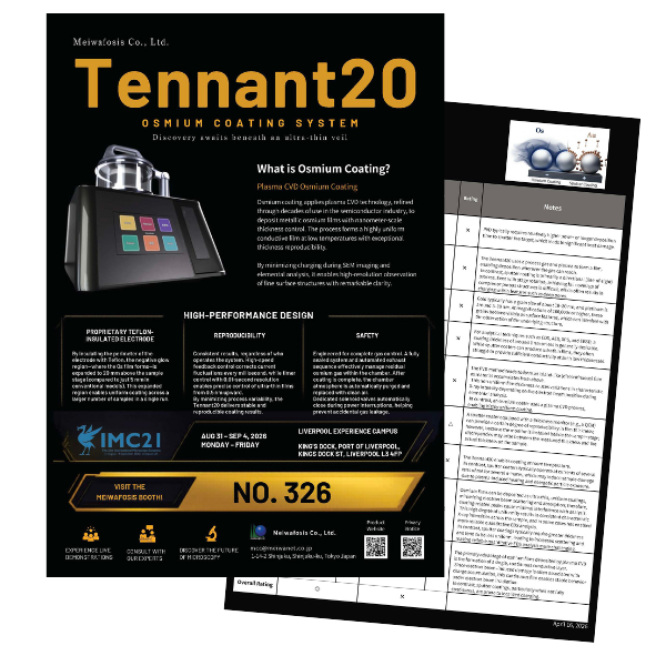
August 31 – September 3, 2026
·
Liverpool Experience Campus, UK
·
Booth 326

See the Tennant20 at Booth 326 and talk with our team about your research applications.

Partner Wanted

Seeking International Sales & Support Partners

We are currently seeking sales & support partners for the Tennant20, with a primary focus on Europe, North America, and Asia. We welcome inquiries from companies with experience in the sales and support of microscopy-related equipment.

Contact Us to Discuss Partnership Opportunities
View the IMC21 Floor Plan
STEP 01
Download Materials

Download comparison sheets and technical specifications to learn more about the Tennant20 and its capabilities.

STEP 02
Request a Demo

Request a consultation, and our team will discuss how the Tennant20 can support your specific research needs.

STEP 03
Get Started

With comprehensive post-installation support, you can quickly start achieving high-resolution SEM imaging with osmium-coated samples.

Contact & Download

Download brochures, technical specifications, and comparison materials, or contact us for more information.

Your data is processed in accordance with the EU General Data Protection Regulation (GDPR) and UK GDPR. You may exercise your rights (access, rectification, erasure, data portability, and objection) by contacting mcc@meiwanet.co.jp.

After submitting the form, you can immediately download the materials from this page.
If you requested a demo, one of our representatives will contact you shortly.